COTS PRODUCTS > COTS DIGITAL / ANALOG PRODUCTS > GPS - PRODUCTS > AT-PMC-GPS
 
Choice of Bus Interface
XMC – x1 Lane PCIe, 2.5Gbps
PMC – PCI bus 32-bit, 33MHz
IRIG-B Time Code Input (Digital)
Optional discrete I/O and IRIG-B
Available in 2 variants –Air Cooled, Conduction Cooled
Four Discrete Inputs & four Discrete Outputs
Rear P16 or Rear P14 or Front I/O available
DIP Switch Configuration provided to control transceivers
On Board GPS Module provided
On Board SMA connector specifically for GPS communication
Optional GPS receiver provided on the card
Front panel connector ( 68 PIN VHDCI ) for easy access to all Ios
8 Serial Communication ports provided
4 ports provide full functionality
4 ports provide half control ( RS232 / RS422 / RS485 )
High-level API for Windows XP, Windows 7 & Linux
 

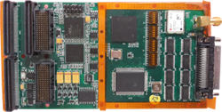
The AT-XMC/PMC-GPS is a slave mezzanine Card which provides x1 Lane PCI-Express interface or 32 bit PCI interface with the host system. It provides interface to host with different types of IO signals for the avionics domain user interactions. The board has an onboard clock, which is kept in sync to either an external time code input or time provided by GPS satellites. Several timing functions are derived from the on-board clock including a programmable periodic pulse rate output ("Heartbeat"), a programmable start/stop output ("Match"), a selectable frequency output ("Oscillator Out", 1 kHz, 1, 5, or 10 MHz) & a time-stamping input ("Time-Tag”).

An onboard IRIG-B time encoder & decoder allow users to accurately synchronize single or multiple modules to a common time source. The card has implemented all its Discrete IO logic in the FPGA. An Octal UART is used to implement serial port functionality. The Card consists of 8 ports of which 4 ports provide full functionality & other 4 provide half control. When configured for RS232 mode a port provides the full set of data & modem control lines. It can also be configured in RS485/RS422 mode. GPS functionality is provided by a receiver built into the antenna housing & communicates to the board via (RS-422) interface.

Software
The AT-XMC/PMC-GPS software includes Drivers & APIs which come with a powerful set of library functions to access the entire SPT functionality. The drivers are designed in a modular fashion consisting of component functions & application functions. The user’s test program can be developed with few calls to the driver by using the set of application functions provided. All data bus functionality is supported by our advanced API (Application Programming Interface). Driver & high-level API libraries for Windows XP, Windows 7 & Linux are available.
Bus Interface
XMC - x1 lane PCIe, 2.5Gbps (PCIe base specification 1.0a)
PMC - 32-bit, 33/66 MHz (PCI 2.2)
Onboard Clock
Synchronization to GPS ±1µs max
Synchronization to time code input ±1µs max
Time base (freewheeling) type
Resolution 1µs
GPS Antenna Cable
Active Antenna
Supply voltage range 3 to 5V
Length 5m
RG174 standard
SMA plug connector
Magnetic base for mounting
GPS Receiver Module
50-channel u-blox 5 engine
No of satellites tracked 16
Acquisition time 32 seconds (typical)
High immunity to jamming
Horizontal position accuracy
Tracking & Navigation -160dBm
Reacquisition -160dBm
Cold start - 144dBm
Max Navigation Update Rate 4 Hz
Velocity Accuracy 0.1m/s
Heading Accuracy 0.5 degrees
Dynamics = 4 g
TIMEPULSE (1Hz Nav) 1 pulse/s, synchronized at rising edge, pulse length 100ms
NMEA Input/Output Protocol supported
SMA Antenna Connector
Time Code input
Format IRIG-B (122)
Modulation ratio 3:1 typical
Input impedance 10KO
Time Code Output
Format IRIG-B(122) (CF & SBS fields not used)
Amplitude (mark) 3.0 Vp-p min, 4.0 Vp-p typical, 6.5 Vp-p max
Modulation Ratio 3:1 (typical)
Discrete I/O
Optional four Discrete Inputs & four Discrete Outputs
Open/GND (Common - break) Discrete Inputs
Open/GND (Common - break) Inputs are diode protected
All Discrete Input Conditioning at TTL Levels, level translated to 3.3V for internal use
Discrete outputs through PhotoMOS relays to switch DC/AC loads
Other I/O’s include
Time Tag Input
Tagged Edge Rising
Rise/Fall Time 150 ns max
Pulse Width (time high) 1 µs min, 999.999 mS max
Time Between Each Rising Edge 500 µs min
Repetition Rate 2000 events/s max
Time Tag Accuracy ± 1 µs
Oscillator Output
Output Off, 1 kHz, 1, 5 or 10 MHz (programmable)
Power-on Default Frequency Off
Output Type Differential RS-422
Wave Shape Square wave, 40% / 60% duty cycle
Recommended Termination 120 O, ½ Watt, line-to-line
Heart Beat Output
Wave Shape Pulse
Pulse Polarity Programmable
Pulse Width 100 ns, 333 ns, 1 µs or 1 ms (Programmable)
Output Current (high or low) 2.5 mA max
Range 200 ns to 65.5 Seconds
Power-on Default Disabled
Match Output
Output Voltage (high) 3.8 V at 4 mA
Output Voltage (low) 0.3 V at -4 mA
Output Current (high or low) ±6 mA max
Setability 1 µs
In-sync output
Output Type Open Collector
External Pull-up Voltage +5 VDC max
Output Voltage (low) +0.5 V max at -20 mA
Output Current (low) -20 mA max
1PPS Output
Single Ended Output
Synchronized to On-Time Edge Rising
Pulse Width 4 µs or 100ms
IO Configurations
IO available on both Front Panel 68 pin VHDCI Connector & Rear Connectors (P14 - PMC or P16 – XMC)
Standard configuration is P16 rear panel I/O
Software Support
Driver & high-level API libraries for Windows XP, Windows 7 & Linux available
Sample applications provided to help users quickly setup & use the card
Physical
Standard Single wide Mezzanine Card form factor confirming to IEEE 1386.1 (74 mm x 149 mm)
Conduction Cooled XMC/PMC Card without Bezel
Environmental
Air-Cooled Conduction-Cooled
Operating Temperature 0ºC to + 60ºC -40ºC to + 85ºC
Power
Primary Supply +5V, +3.3V, +12V & -12V from PMC Connectors when configured as a PMC Card, +3.3V & all other voltages internally derived
Primary Supply +3.3V, +12V & -12V from XMC Connectors when configured as XMC Card, all other voltages internally derived
Warranty
1 year limited warranty
 
CORPORATE   ABOUT   FOLLOW US ON
AdTEC Electronics Inc.
4677 Old Ironsides Drive
Ste 230
Santa Clara, CA 95054
USA
 
AdTEC Electronics specializes in providing end-to-end custom product design & development encompassing System, Mechanical, Board Electronics, Chip design, Firmware and Application Software Engineering. Our design capabilities include design for testability and rugged design to meet both commercial and stringent regulations.
 
HOME ABOUT US COTS PRODUCTS SERVICES & SOLUTIONS SUPPORT & RESOURCES NEWS & EVENTS BLOG CONTACT US
AdTEC Electronics Inc.